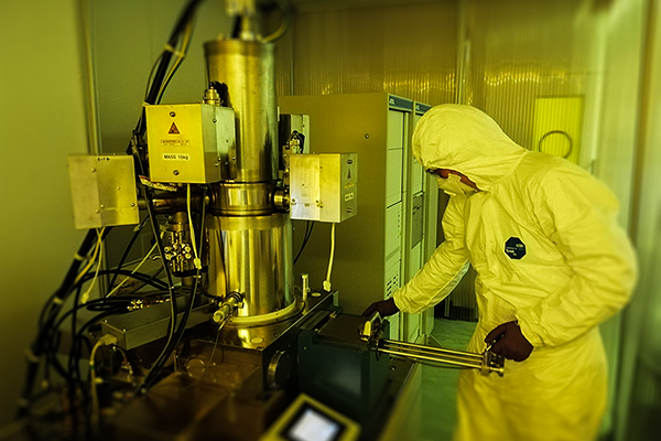
We carry out nanofabrication in the Denys-Wilkinson cleanroom where we have access to a suite of cutting-edge equipment. The main lithography tool used in our work is the JEOL JBX-5500FS electron-beam lithography system. With this system it is possible to reliably fabricate structures with feature sizes well below 100 nm. The system has an interferometer-controlled stage which allows for the possibility of writing of nanoscale patterns across large substrates with a stitching accuracy better than 15 nm. The electron beam is generated by a ZrO/W emitter and is focussed via a four-stage electron lens system which allows beam currents between 100 pA to 40 nA. The system can be operated with acceleration voltages between 25 kV and 50 kV.

The main focus of our work is in the fabrication of graphene molecular transistors which we produce using a negative EBL process and plasma etching on CVD grown graphene. For these devices, electron-beam lithography is used to pattern nanoconstrictions into the graphene sheet. This step is aligned with prefabricated source, drain and gate electrodes already on the chip. The resulting graphene constrictions can then be subsequently electroburnt using an automated feedback-controlled procedure to produce extremenly small nanogaps similar in size to that of single molecules. Scanning electron microscope images of some of the patterned devices are shown below.
In addition to electron-beam lithography, our group has skills using a variety of cleanroom techniques which include photolithography, nanoimprint lithography, wet and dry etch processes as well as wire-bonding. In addition, we also have skills in the deposition and etching of thin-films as well as the characterisation of patterned nanostructures. For this we use high resolution scanning electron micropsy (SEM) and atomic force microscopy (AFM).
We also have projects which aim to measure thermoelectric effects at the nanoscales. To do this we have incorporated heaters and thermometers into our graphene nanogap transistors. Fabrication of these devices is carried out in a series of steps, each of which require accurate alignment with the previously defined features. A microscope image of a completed device is shown below.
Recently we have demonstrated the very high resolution of the EBL system by directly patterning graphene nanogap devices. To do this requires careful calibration of the EBL optics to ensure that the beam has the smallest possible spot size when writing on the sample surface. Two of the patterned nanogap devices are shown below. A sacreficial chromium etch mask is used to transfer the nanogap into a layer of PVD graphene via oxygen plasma etching.
Below is the group logo fabricated using UV lithography. UV lithography is carried out using a state-of-the-art suss MJB4 manual mask aligner. Such a tool allows for rapid patterning of entire wafer substrates with a resolution below 5 μm being readily achievable.