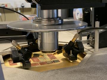
One of the key necessities for performing measurements on graphene single molecule or nanoribbon devices is the ability to reliably produce and characterise large numbers of graphene electrodes. For this we have developed our own electroburning procedures which we run on an automated Cascade Microtech probe station. Our measurement system can incorporate a variety of source-measurement equipment. For low-noise DC measurements we use a variable gain FEMTO DLPCA-200 current amplifier with an Adwin-Gold II real-time data acquisition system and analog voltage source. We also use a home-made voltage multiplier which can apply up to 120 V on a global wafer back-gate.

After the fabrication of a nanogap device is complete, wirebonding is used to connect the contact pads on the chip with bond pads on the sample holder or printed circuit board. Thin gold or aluminium wire (0.025 mm in diameter) is bonded by application of an ultra-sonic pulse and compression applied via a metal wedge. The completed chip can then be mounted in one of our Triton dilution fridges for low temperature transport measurements.
As well as characterisation at ultra-low temperatures, we also have access to dip-stick and cryocooler based "puck tester" systems. Once devices have been characterised at room temperature and wire bonded, the samples can be cooled rapidly to cryogenic temperatures and electrically characterised. Our puck tester systems also incorporate a superconducting magnet enabeling magnetic characterisation of the devices. Together these systems enable robust characterisation of many hundreds of fabricated nanodevices both before and after the electroburning process and after molecule or nanoribbon incorporation into the nanogap.