
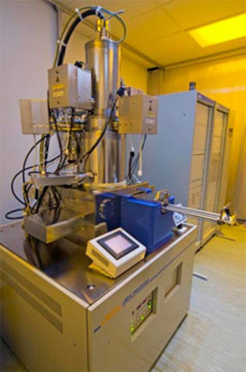
Litography
The tables below list the accelerating voltages available in the four operating modes, together with the maximum field sizes and minimum scanning steps. Fields can be stitched together to write a whole wafer using a translation stage. The stage moves in a step-and-repeat mode guided by an optical interferometer. The specified stitching accuarcy is better than 40nm, although the system outperforms this (see section on performance below). The specified minimum linewidth is < 10nm, with 9.8nm being achieved.
e-beam writing times
| e-beam mode | Accelerating voltage | Objective lens | Maximum field size |
|---|---|---|---|
| 1 | 25 kV | Fourth lens | 2mm x 2mm |
| 2 | 50 kV | Fourth lens | 1mm x 1mm |
| 3 | 25 kV | Fifth lens | 200 μm x 200 μm |
| 4 | 50 kV | Fifth lens |
100 μm x 100 μm |